|
|
| |
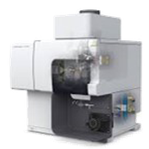 |
Agilent 5100 DVD Inductively Coupled Plasma-Optical Emission Spectrometer |
|
Hourly Rate : $35 |
Used to quantify the elements in a sample. Typical concentrations of 1-100ppm. Radial or Axial view emission spectrometer. Autosampler. |
| |
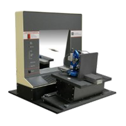 |
Back Reflection Laue Diffractometer |
|
Hourly Rate : $51 |
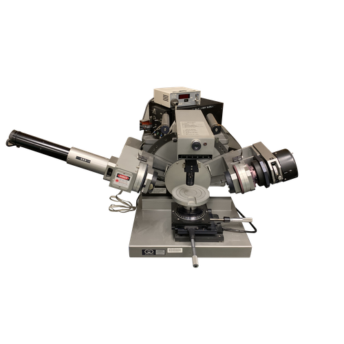
This system uses a two-dimensional multiwire detector to collect back-reflection Laue patterns to determine the orientation of large single crystals and thin film single crystal substrates. |
| |
 |
Bruker D8 GADDS Multipurpose Diffractometer |
|
Hourly Rate : $51 |
The Bruker General Area Detector Diffraction System (GADDS) instrument permits collection of diffraction data over a 2theta range -15 to 117 degrees and a chi (tilt) range as large as 30 degrees. The Eulerian � cradle, which permits many unique tilts and rotations of the sample, with a very fast two-dimensional area detector. This configuration makes this instrument ideal for texture and stress measurements, as well as traditional XRPD and limited SCD and GIXD. A selectable collimator, which conditions the X-ray beam to a spot with a size from 0.5mm to 0.05mm diameter, combined with a motorized x-y stage permits micro-diffraction for multiple select areas of a sample or mapping across a sample's surface. Samples can include thin films on wafers or dense pieces up to 6" in diameter (maximum thickness of 3 mm), powders in top-loaded sample holders or in capillaries, dense pieces up to 60mm x 50mm x 15mm (and maybe even larger). In addition, the GADDS system can collect basic WAXS, SAXS, and GISAXS data by configuring the instrument with a collimator-mounted or detector-mounted beam stop and a helium purged flight tube to reduce air scatter. |
| |
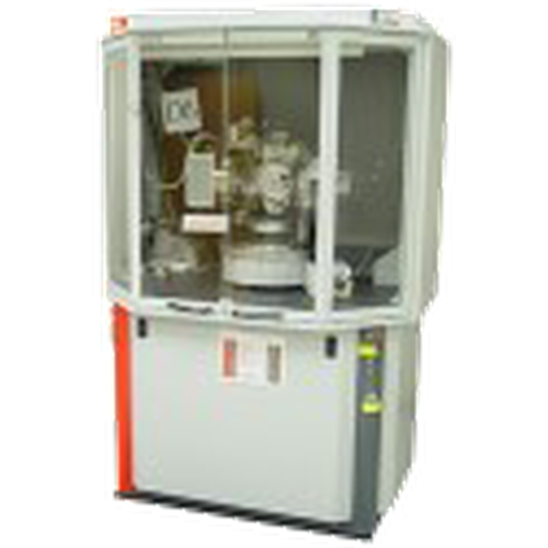 |
Bruker D8 High Resolution Diffractometer |
|
Hourly Rate : $51 |
Uses a conventional 1.6kW sealed tube copper anode, and the X-rays are reflected off a parabolic graded multilayer mirror to produce a parallel beam. This instrument features a four-bounce Ge (022) incident beam monochromator. This optic produces highly monochromatic X-rays, eliminating all incident wavelengths except Cu Kα1 (λ =1.540562 �). The goniometer is a chi-cradle type, with full phi axis rotation and x-y-z translation. Including omega, this gives six positioning axes for the sample (not including the detector axis, 2Theta). Two detectors are mounted on this instrument: a point detector, which offers higher resolution at the cost of speed, and a faster but lower-resolution linear position-sensitive detector. Popular applications include HRXRD, reciprocal space maps (RSM), and XRR. |
| |
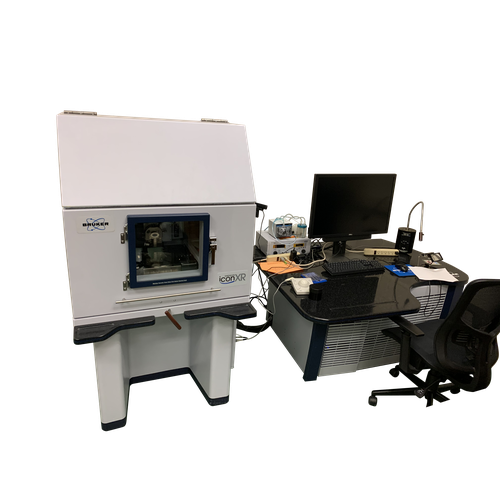 |
Bruker Dimension Icon SPM |
|
Hourly Rate : $44 |
The Icon XR has many SPM modes including contact and PeakForce tapping mode with ScanAsyst, Magnetic Force Microscopy, Piezo Force Microscopy, conducting atomic force microscopy (AFM). There are also additional features such as electrical characterization from 80 fA to 1 uA with 10 nm spatial resolution, Kelvin Force Probe Microscopy with amplitude or frequency feedback, and pixel-by-pixel quantitative force characterization to probe material properties. |
| |
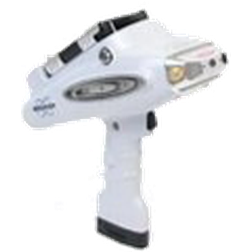 |
Bruker Tracer-III SD Portable XRF |
|
Hourly Rate : $51 |
This energy dispersive X-ray fluorescence (ED-XRF) unit provides rapid qualitative non-destructive elemental analysis. It features a rhodium X-ray source and a silicon-based detector and is capable of identifying most elements heavier than magnesium in three minutes or less with a spectrum from 1-40 keV. Normally it gives qualitative results, e.g. trace element identification and relative comparisons of similar samples. Quantitative analysis is possible but more difficult, because the user must create a set of calibration standards for each element of interest. |
| |
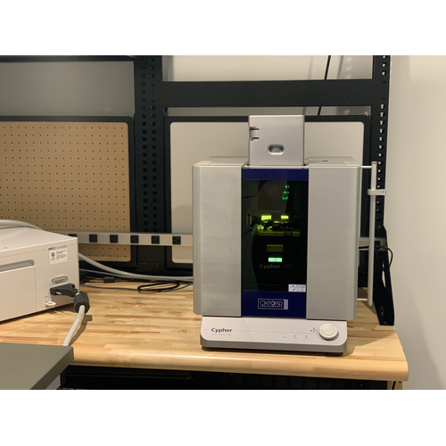 |
Cypher VRS AFM |
|
Hourly Rate : $35 |
The Cypher VRS AFM is a full-featured video-rate AFM capable of measuring insitu nanoscale dynamic processes at video-rate speeds including particle conformational changes, formation and macromolecular assemblies, and many other dynamic processes that are difficult to trace and analyze with conventional approaches. The AFM offers high-resolution video-rate imaging at up to 625 lines per second, which results in up to 10 frames per second. This tool can process imaging during heating/cooling/biasing as well as imaging of liquids. Cypher is well-suited for EFM, KPFM, MFM, LFM, PFM, force mapping and tapping mode. |
| |
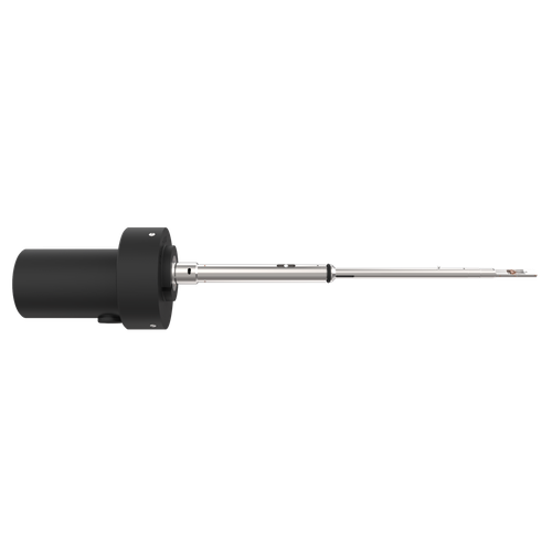 |
DENS Lightning In situ heating/biasing holder for Themis Z |
|
|
The Sample Holder is the critical element connecting the Nano-Chip with the microscope and provides researchers with the ability to measure pico amps and apply high voltages up to 150 volts, all within a heated environment (up to 1200 �C). Made from titanium for its optimal mechanical stability, the double tilt Sample Holders provide in situ researchers with the widest application space. |
| |
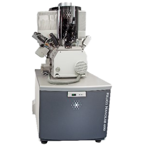 |
FEI Helios Nanolab 600 Dual Beam System |
|
Hourly Rate : $94 |
Configured to carry out nano-scale characterization and nano-machining on a wide-range of materials from various study areas such as biotechnology, and materials and energy research. This instrument has magnetic immersion electron optics to give 0.9 nm resolution at 15kV. A high brightness field electron emitter can deliver a beam current up to 22 nA and the accelerating voltage from 350V to 30kV. The ion optics produces a resolution of 5.0 nm at 30KV and liquid Gallium emitter delivers 20 nA ion current and the voltage ranging from 0.5 kV to 30kV. |
| |
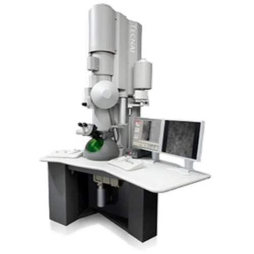 |
FEI Tecnai Multipurpose Digital TEM |
|
Hourly Rate : $70 |
The FEI Tecnai (G2 Spirit TWIN) is a high quality 120 kV multipurpose TEM, providing high resolution and good contrast. The high-resolution TWIN lens allows for imaging at both moderate and high magnification up to 0.36 nm point-to-point resolution & 0.2 nm lattice resolution. The digital TEM combines excellent performance with optimized ease-of-use for high resolution imaging, elemental analysis and mapping. |
| |
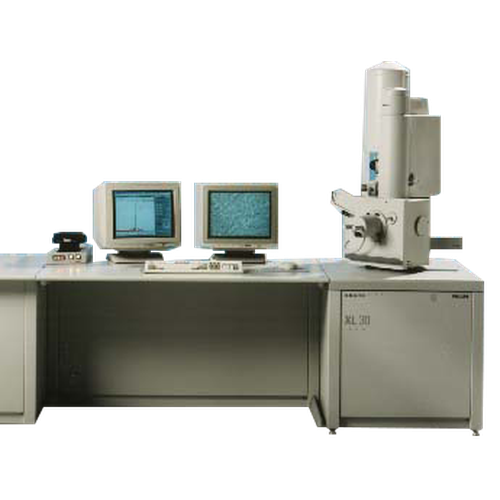 |
FEI/Philips XL30 FEG ESEM |
|
Hourly Rate : $70 |
A high performance, extremely flexible and well-equipped microscope for general-purpose microscopy, low-vacuum and environmental scanning microscopy (ESEM). It is also equipped with a Peltier stage. Resolution at 30KV is 3.5 nm. The minimum magnification is about 20x. |
| |
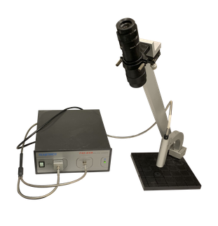 |
Filmetrics Reflectometer |
|
Hourly Rate : $37 |
Spectroscopic reflectometry is used to determine the thickness and complex index of refraction (n & k) of thin films, by comparing the spectral amplitude and periodicity of light reflected at normal incidence from a thin film surface with light reflected from a known reference sample, and fitting the result to a mathematical model based upon proposed values for the parameters thickness, n and k.
MIT MRSEC's reflectometer has been optimized to enhance the spectral yield in the near-IR, with a consequent spectral range from 480 to 1700 nm. The measurable film thickness range is from about 100 nm to 25 �m, and the accuracy is +/-10 � or 0.4%, whichever is larger.
The reflectometer has a large-sample stage with a spot size on the order of 1 mm. |
| |
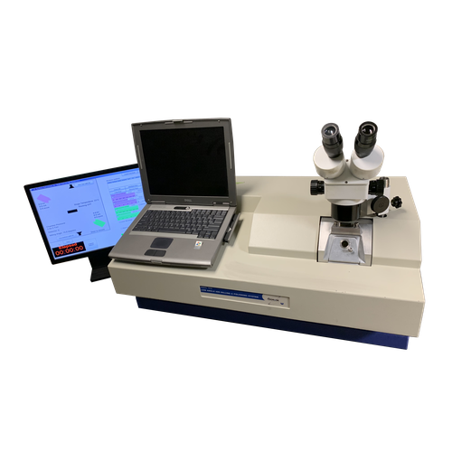 |
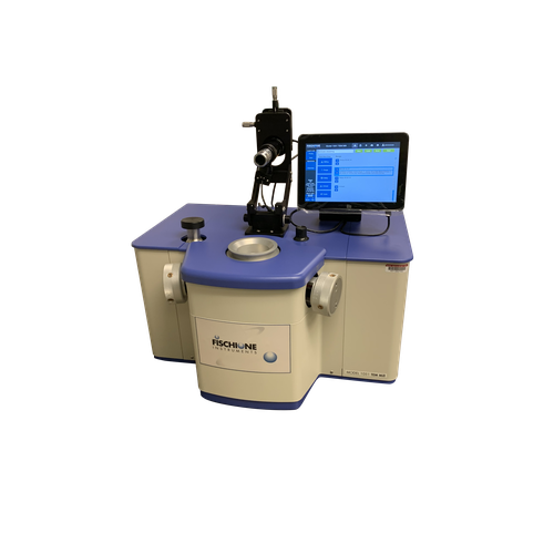
Fischone 1010 Ion Mill |
|
Hourly Rate : $9.26 |
The EM lab offers various equipment for specimen preparation with different techniques.
Fischione 1010 Ion Mill
Fischione 1051 TEM Mill
Precision Ion Polishing System (PIPS)
Fischione 170 Ultrasonic Cutter
EMS Q150T ES coater
For RMC MT-X cryo-ultramicrotome |
| |
 |
Fischone 1051 TEM Ion Mill |
|
Hourly Rate : $9.26 |
The EM lab offers various equipment for specimen preparation with different techniques.
Fischione 1010 Ion Mill
Fischione 1051 TEM Mill
Precision Ion Polishing System (PIPS)
Fischione 170 Ultrasonic Cutter
EMS Q150T ES coater
For RMC MT-X cryo-ultramicrotome |
| |
 |
Four Point Probe PRO4-4M00 |
|
|
The Pro4 four point probe can measure the sheet resistivity of semiconductors, a variety of material research measuring thin films on a variety of substrates, and is designed to meet the demands of research on wafers, thin films, solar cells and a variety of applications. Attached permanently to Keithley 2601B. |
| |
 |
Gaertner Scientific 3-Wavelength Variable Angle Ellipsometer |
|
Hourly Rate : $37 |
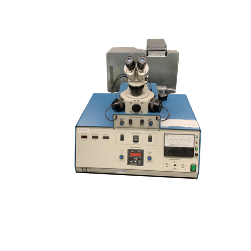
Ellipsometry is used to determine the thickness of thin films and to find the complex index of refraction (n & k) of materials, by analyzing the polarization of light reflected at an angle from a sample surface. MIT MRSEC's ellipsometer probes the sample with a single wavelength laser, with a wavelength of red (633 nm). The analysis area is about 1 mm x 3 mm. The minimum measurable film thickness is a few �ngstroms with an accuracy of +/- 3 �, and the maximum measurable thickness is about 10 �m. |
| |
 |
Gatan Precision Ion Polishing System (PIPS) |
|
Hourly Rate : $9.26 |
The EM lab offers various equipment for specimen preparation with different techniques.
Fischione 1010 Ion Mill
Fischione 1051 TEM Mill
Precision Ion Polishing System (PIPS)
Fischione 170 Ultrasonic Cutter
EMS Q150T ES coater
For RMC MT-X cryo-ultramicrotome |
| |
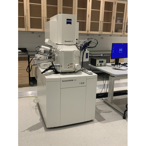 |
Gemini 450 SEM |
|
Hourly Rate : $55 |
The Gemini 450 SEM, from Zeiss, is a field emission scanning electron microscope. The instrument combines ultrahigh resolution imaging with the capability to perform advanced analytics while maintaining flexibility and ease-of-use. It's equiped with Everhart Thornley Secondary Electron Detector, Inlens Secondary Electron Detector, Inlens Energy Selective Backscatteres�Electron Detector (EsB), High efficiency Variable Pressure Secondary electron�Detector (VPSE),Angular selective Backscattered Detector, Annular STEM Detector (aSTEM4) and Oxford AZtec 100 EDS Detector. |
| |
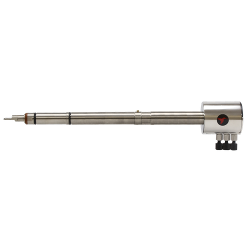 |
Hummingbird Scientific Liquid flow / electrical biasing holder |
|
|
Gen-IV Liquid-Electrochemistry TEM holder tip for FEI/TFS TEM
- Continuous flow: The holder assembly includes tubes to introduce liquid with a syringe pump so that
the sample can be exposed to a continuous flow of liquid or the liquid composition can be changed.
- Electrochemistry: The holder enables electrochemical stimuli through the use of patterned window
chips with integrated electrodes connected to an external potentiostat.
- Heating: The holder accepts window chips with integrated heating elements so that the liquid medium
can be heated to its boiling point or 100�C. |
| |
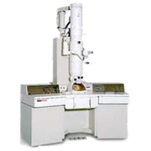 |
JEOL 2010 Advanced High Performance TEM |
|
Hourly Rate : $70 |
This instrument is an advanced, digitally controlled dedicated transmission electron microscope operating at 200KV with a lanthanum hexaboride cathode. It is capable of an ultimate point-to-point resolution of 0.19 nm, with the ability to image lattice fringes at 0.14 nm resolution. |
| |
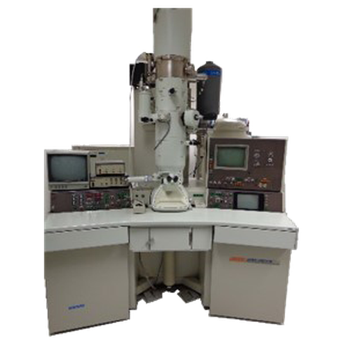 |
JEOL 2010 FEG Analytical Electron Microscope |
|
Hourly Rate : $70 |
A multipurpose high resolution analytical electron microscope with high resolution image quality and high analytical performance, EDS X-ray analysis. The system is also equipped with a Gatan image filter (GIF) for EELS and energy filtered imaging, and a scanning image observation device (ASID), and 3 CCD cameras for various applications. |
| |
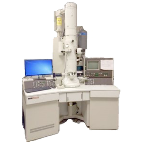 |
JEOL 2011 High Contrast TEM |
|
Hourly Rate : $70 |
A high performance TEM with advanced features and functions. The electron gun allows high-brightness with filament-saving low emission current. Other features include friendly controls, automatic filament heating, high tilting 60 degree single tilting holder, cryo objective lens polepiece for characterizing soft materials, AMT digital imaging camera, and a transmission catholuminescence attachment. |
| |
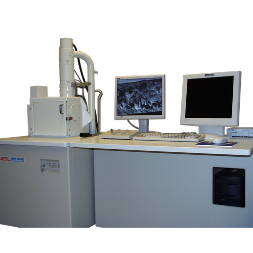 |
JEOL 5910 General Purpose SEM |
|
Hourly Rate : $40 |
A general purpose digital SEM, with the following attributes: very easy to use, remotely accessible via the web, Bruker EDX system for elemental analysis and mapping, and NPGS system for electron beam lithography. |
| |
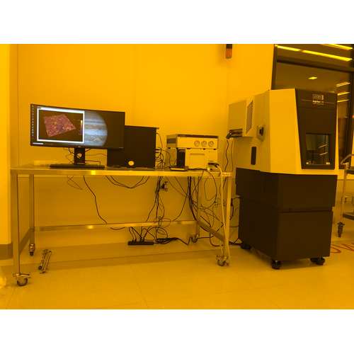 |
Jupiter XR AFM |
|
Hourly Rate : $70 |
The Jupiter XRM AFM is high speed and high resolution AFM with a fully-addressable stage that can reach any point on samples up to 200 mm in diameter. Extended-range scanner provides large 100 _m X-Y & 12 _m Z scan range. Jupiter XRM AFM is well-suited for multifrequency modes, such as Dual AC and AM-FM. Other techniques include EFM, KPFM, MFM, LFM, force spectroscopy and tapping mode. Jupiter is located in the MIT.nano cleanroom facilities. |
| |
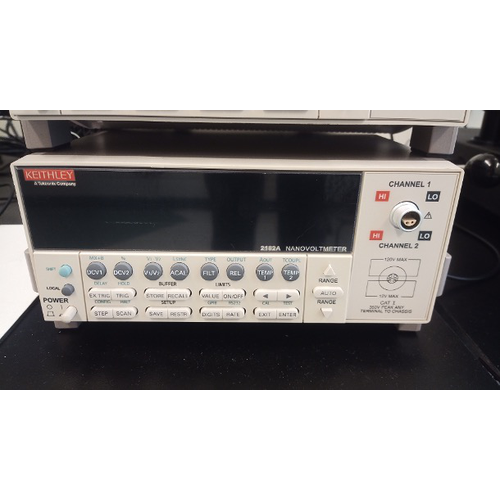 |
Keithley 2182A Nanovoltmeter |
|
|
The Model 2182 is a 71⁄2-digit high-performance digital nanovoltmeter. It has two input channels to measure voltage and temperature. |
| |
 |
Keithley 6221 DC and AC Current Source |
|
|
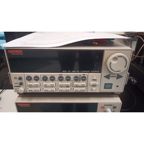
The Model 6221 AC and DC Current Source combines ease of use with exceptionally low current noise. High sourcing accuracy and built-in control functions make the Model 6221 ideal for applications like Hall measurements, resistance measurements using delta mode, pulsed measurements, and differential conductance measurements. |
| |
 |
Keysight/Agilent/HP 8753C Network Analyzer |
|
|
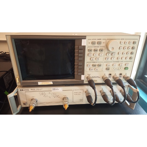
The 8753C is a high performance vector network analyzer for laboratory or production measurements of reflection and transmission parameters. It has an attached 85047A S-parameter test set. |
| |
 |
Linkam Temperature Controlled Microscope Stage (FTIR600 & THMS) |
|
Hourly Rate : $20 |
This stage is availabe for use on all the microscopes in the lab. Temperature Range: (-196 C) thru 600 C. |
| |
 |
Mass Balances |
|
Hourly Rate : $48 |
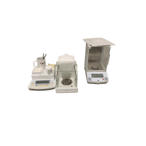
Satorius Microgram sensitivity |
| |
 |
NVision 40 Cross Beam System |
|
Hourly Rate : $70 |
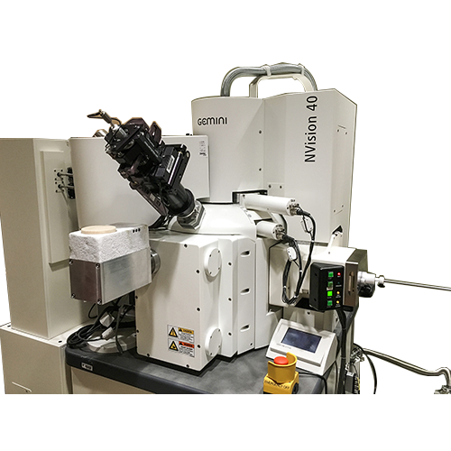
The NVision 40 CrossBeam� Focused Ion Beam (FIB) system can be used to conduct characterization, milling and deposition at the nano-scale. The NVision 40 consists of a high-resolution Zeiss Gemini� electron beam column coupled with a Zeiss Zeta Ga ion beam and gaseous injection system (GIS).� The secondary electron imaging has a resolution of 1.0nm at 15kV and 1.4nm at 1kV. The Ga ion beam has an energy range from 1 to 30 kV and a probe current from 1 pA to 45 nA, which can achieve a resolution of 4.0nm for both imaging and milling.� Currently, the GIS is configured with C and Pt depositions and complemented by an Omniprobe 300 to allow FIB lift-out for TEM sample preparation. |
| |
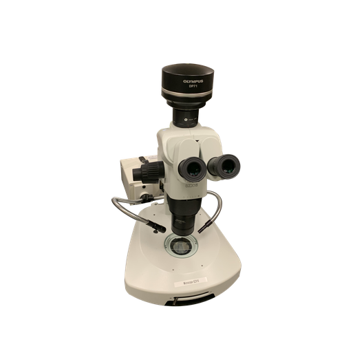 |
Olympus Stereo Microscope SZX16 |
|
Hourly Rate : $30 |
Reflectance, Transmission Brightfield, Darkfield, Polarization, Digital Camera, Software. |
| |
 |
Panalytical Multipurpose Diffractometer |
|
Hourly Rate : $51 |
This diffractometer can be used to collect XRPD, GIXD, XRR, and residual stress data. Some texture analysis is also possible. Sample sizes may be as large as 60mm diameter by 3-12mm thick, though a more typical sample size is 10-20mm diameter. Data collection modes can be changed between high-speed high-resolution divergent beam diffraction and parallel beam diffraction. There are several accessories for this instrument, including an X'Celerator position sensitive detector, a furnace for in-situ high temperature measurements, a cryostat for in-situ low temperature measurements, a diffracted beam monochromator, and a 15-position automatic sample changer. |
| |
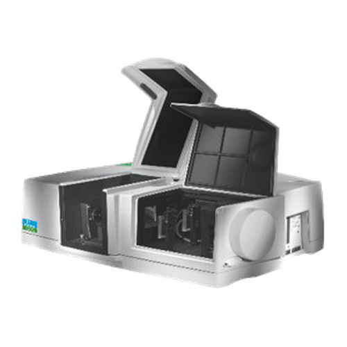 |
Perkin Elmer Lambda 1050 UV/VIS/NIR Spectrophotometer |
|
Hourly Rate : $37 |
Used to measure the Transmittance, Reflection or absorbance of a sample. Measurement Range: 175nm to 3300nm. Integrating Sphere. |
| |
 |
PHI VersaProbe II |
|
Hourly Rate : $44 |
X-ray photoelectron spectroscopy (XPS, aka ESCA) permits elemental and chemical spectroscopic analysis of both conductive and insulating samples, with high depth resolution (10 nm or less), good elemental sensitivity (0.1 to 0.01 atomic percent), and lateral resolution down to 10 �m. Changes in elemental composition with depth (to a maximum depth of about 10 nm) can be documented nondestructively by recording surface composition while varying sample tilt relative to the analyzer (this technique is called angle-resolved depth profiling). Compositional changes with depth down to a few hundred nm can be observed by recording surface composition while using an ion gun to gradually remove surface layers. The spatial distribution of elements or chemistries on a surface can be mapped with a lateral resolution of down to ten microns. The sample is analyzed in an ultra high vacuum chamber.
MIT MRSEC's PHI Versaprobe II XPS has a C60 cluster-ion gun as well as a floating voltage argon single-ion gun for depth profiling. The cluster-ion gun permits depth profiling softer materials which would be too damaged by single-ion bombardment. Other features of this XPS are a portable transfer vessel so that processed samples can be loaded into the XPS without exposure to air; an in situ heat/cold stage (-120C to 500C); and X-ray induced secondary electron imaging (SXI), which aids significantly in setting up for small area analysis. |
| |
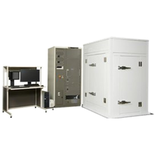 |
Physical Electronics Model 700 Scanning Auger Nanoprobe |
|
Hourly Rate : $44 |
A scanning Auger microscope can be thought of as a scanning electron microscope with a specialized electron energy analyzer attached. Auger electron spectroscopy permits elemental and sometimes chemical analysis with high depth resolution (about 3 nm), good elemental sensitivity (1.0 to 0.1 atomic percent) and high lateral resolution (minimum 11 nm). The spatial distribution of elements on a surface can be mapped. Changes in elemental composition with depth can be documented by recording surface composition while using an ion gun to gradually remove surface layers. The sample is analyzed in an ultra high vacuum chamber.
MIT MRSEC's PHI Model 700 Nanoprobe has a field emission electron source for high lateral resolution; a floating voltage argon gun for depth profiling and sample neutralization; a portable transfer vessel so that processed samples can be loaded into the instrument without exposure to air; and a nitrogen-coolable impact fracture stage for in situ preparation of intergranular fracture surfaces for analysis. |
| |
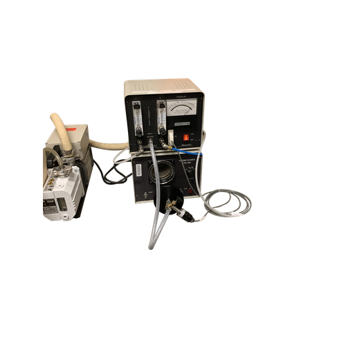 |
Plasma Cleaning |
|
Hourly Rate : $37 |
Oxygen and Nirogen. |
| |
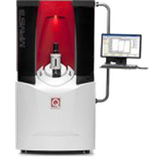 |
Quantum Design Inc. Magnetic Property Measurement System (MPMS-3) |
|
Hourly Rate : $10 |
This apparatus is capable of measuring magnetic moments in the range +/-2 emu to a resolution of 10-7 emu. Measurements may be obtained in the temperature range 1.8 to 400 K with magnetic fields from -7 Tesla to +7 Tesla. The system is fully automated, accepting flexible user-programmed parameters that allow for unattended operation day and night. |
| |
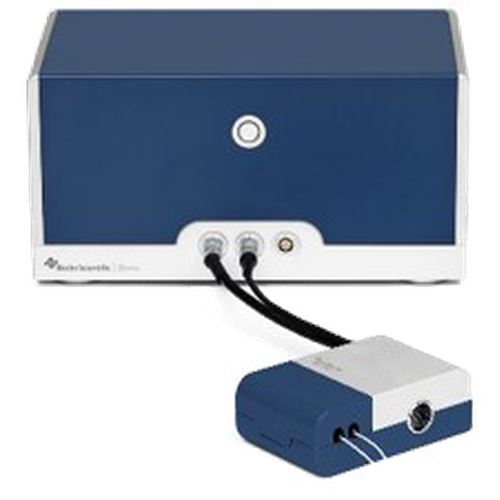 |
Quartz Crystal Microbalance with Dissipation, QCMD |
|
Hourly Rate : $33 |
The QCM-D is used to study molecular interactions and surface science.
Based on a vibrating quartz crystal sensor (an acoustic resonator). Measurements are made based on changes in vibration frequency in response to reactions that occur on the sensor surface. The measurements provide answers about mass and structural changes at the nanoscale level.
Common applications include measurements on proteins, polymers, surfactants and cells onto surfaces in liquid.
Measurement Cells available: Flow, static, window, electrochemistry and humidity. |
| |
 |
Reichert |
|
Hourly Rate : $37 |
Transmission, Reflectance, Bright Feld, Dark Field, Oblique. |
| |
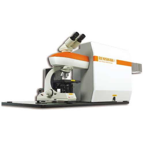 |
Renishaw Invia Reflex Micro Raman |
|
Hourly Rate : $37 |
Microscope based raman system with three laser excitation and spectrometer with CCD detector. Motorized stage and software allows mapping or imaging. Temperature controlled microscope stage. Automated polarization. Open Sample compartment. Photoluminescence. Low wavenumber gratings. |
| |
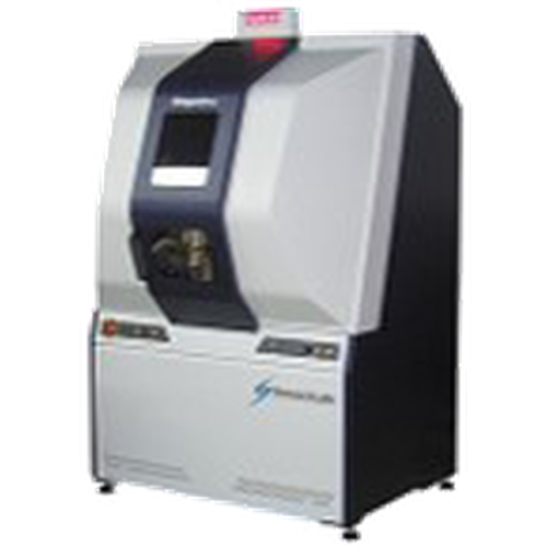 |
Rigaku Smartlab Multipurpose Diffractometer |
|
Hourly Rate : $51 |
This diffractometer features a 9kW rotating anode X-ray source, which produces a much higher intensity beam than sealed tube anodes. It is capable of performing most common XRD measurements as well as many uncommon ones, and can rapidly switch between various optical configurations including both Bragg-Brentano and Parallel-Beam geometries. It is suited for XRPD, XRR, GIXD, HRXRD, reciprocal space maps (RSMs), in-plane pole figures, and in-plane grazing incidence XRD scans. Accessories for this instrument include:
Incident-beam Ge (022) double bounce monochromator, diffracted-beam graphite monochromator
D/teX Ultra linear position sensitive detector furnace, capable of heating to 1400�C in air, inert gases, or vacuum
Capillary stage used to hold and spin capillaries of various diameters for data collection in transmission mode
Battery cell designed to charge and discharge Li-ion based battery materials in-situ.
In-plane arm which allows the point detector to traverse more than a quarter hemisphere around the sample |
| |
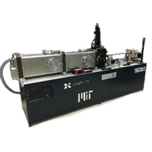 |
SAXSLAB Small Angle X-ray Scattering System |
|
Hourly Rate : $51 |
The SAXSLAB instrument is setup to perform transmission small or wide angle X-ray scattering on freestanding samples, powders prepared in kapton tape, liquids in disposable or resealable capillaries, gels in sandwich cells with mica windows. Also, there is capability to perform grazing incidence small or wide angle X-ray scattering (GI-SAXS/WAXS) on nanostructured surfaces. The instrument uses a Rigaku 002 microfocus X-ray source with an Osmic staggered parabolic multilayer optics to focus the beam crossover at the second pinhole. It has two sets of JJ X-ray 4 jaw collimation slits that are tunable from 0.02 to 1 mm and are made of single crystal to reduce slit scattering effects. Samples are introduced into a large vacuum chamber that is pumped down to 0.08 mbar. The sample stage has x-y travel and theta tilt for grazing incidence SAXS measurements. The DECTRIS PILATUS 300K detector has the apability of automatically moving from 100 mm to 1500 mm depending on the izes that are indented to be probed; for WAXS (3-70 �) and for SAXS (30-2300 �). |
| |
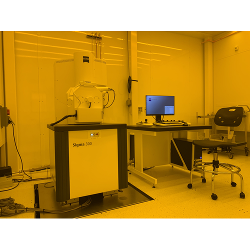 |
Sigma 300 SEM |
|
Hourly Rate : $55 |
Zeiss Sigma 300 SEM is a high-resolution scanning electron microscope located in the MIT.nano cleanroom facilities. It's equiped with Everhart Thornley Secondary Electron Detector and Inlens Secondary Electron Detector. SIGMA 300 is capable of reaching resolution of 0.8 nm at 15KV and 1.2 nm at 1 kV with in-lens secondary electron detector. |
| |
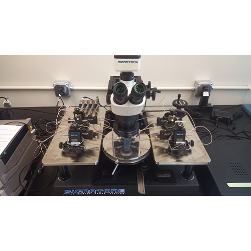 |
Signatone Probe Station S-1160 |
|
|
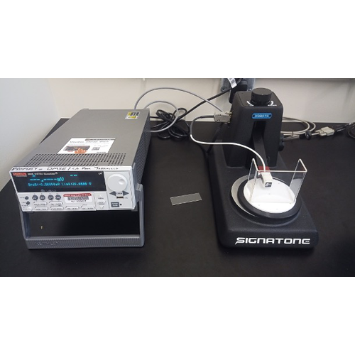
150mm - 200mm Manual Probe System designed for reliable and accurate analytical testing of DC, CV-IV, and High-Power applications.
Additional equipment:
40A microwave probe uses low loss coaxial techniques to achieve an insertion loss of less than 0.8 dB and a return loss of greater than 18 dB through 40 GHz.
Precision Premier II Ferroelectric tester is capable of executing a single pass hysteresis loop in 100μs with no interlacing of the data acquisition. The capture rate for the 18bit ADCs in the system is 2MHz. The maximum hysteresis frequency of the Premier II is 250kHz. |
| |
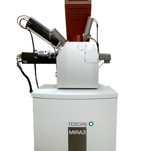 |
Tescan MIRA3 SEM |
|
Hourly Rate : $70 |
In situ scanning electron microscopy characterization facility (ISCF) is formed to enable two specific types of experiments that can rarely be carried out in other MRL microscope facilities: (i) in situ SEM-based experiments (using wide range of miniaturized setups for mechanical loading, heating/cooling, hydrogen-charging, etc.); and (ii) long-duration SEM scans (e.g. overnight EBSD scans). ISCF is managed and operated by the Tasan Group (DMSE, MIT). The group is (i) maintaining the scanning electron microscope, its detectors, accessories, in-situ setups; (ii) developing new tools, methods and expertise (sometimes in collaboration with other groups); (iii) providing support to external users. |
| |
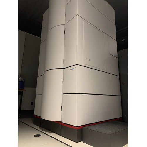 |
Themis Z STEM |
|
Hourly Rate : $87.5 |
The Thermo Fisher Scientific (TFS) Themis Z G3 aberration-corrected scanning transmission electron microscope (STEM) achieves < 0.6 � resolution and is equipped with an optimized monochromator for < 30 meV energy resolution at 60 kV, a Gatan Continuum electron energy loss spectrometer and image filter, a TFS Super-X energy dispersive x-ray spectrometer system, a segmented STEM detector for fast DPC and iDPC imaging, a Lorentz lens, a 16 megapixel Ceta II camera with 300 fps capture rate, and a 4D STEM EMPAD camera. Single tilt, double tilt, and tomography holders are available. The instrument can be operated at 60, 200, and 300 kV for the flexibility to accommodate a range electron beam sensitive materials. |
| |
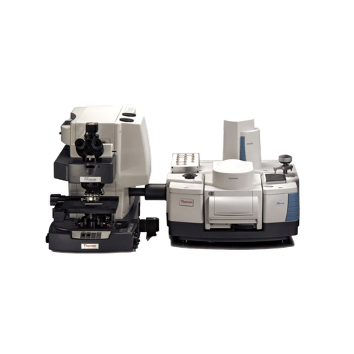 |
Thermo Fisher Continuum Fourier Transform Infrared Microscope |
|
Hourly Rate : $33 |
This is an FTIR microscope that is attached to the FTIR6700 bench. An FTIR spectra can be collected from spot sizes down to 20um (Typical is 100um). Data can be collected in Transmission, Reflection, Emission or Attenuated Total Reflection mode. This microscope is capable of FTIR mapping and ATR mapping. |
| |
 |
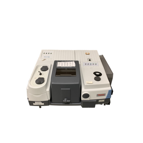
Thermo Fisher FTIR iS50 Fourier Transform Infrared Spectrometer |
|
Hourly Rate : $33 |
FTIR spectrometer�with a fully-automated multi-spectral range system that can acquire spectra from far-infrared to visible (12,500 � 50 cm-1) with automatic range switching. You can initiate novel integrated diamond attenuated total reflection (ATR) modules at the touch of a button, enabling access to these techniques without manually changing system components with a range of (5000 � 100 cm-1). Other options are transmission, reflection ATR, polarization, emission & time dependent modes. |
| |
 |
Thermo Fisher FTIR6700 Fourier Transform Infrared Spectrometer |
|
Hourly Rate : $33 |
This is an FTIR bench with available detectors, beam splitters and sources to allow data collection in the near, mid and far IR. Accessories are available that allow for Transmission, Reflection or Attenuated Total Reflection (ATR) measurements. |
| |
 |
Veeco Dimension 3000/3100/MultiMode |
|
Hourly Rate : $44 |
Scanned probe microscopy (SPM) uses a tiny mechanical probe to record sample surface topography and explore forces between the probe tip and sample surface on a very fine spatial scale, tracking the surface with nanoNewtons of force or less. Vertical resolution is in the sub-nanometer range, and lateral resolution is typically in the nanometer range (limited by the probe radius). Magnetic and electrostatic domains, hydrophilic/hydrophobic regions, and other variations in surface property can be mapped along with surface topography. Electrical characterization and force characterization on the nanoscale can also be performed.
MIT MRSEC has two SPM controllers and three SPM microscopes which can be used together in various configurations.
Veeco/Digital Instruments Nanoscope IIIa Scanned Probe Microscope Controller with Dimension 3000 SPM. The Dimension 3000 is a large stage microscope operable in many SPM modes, with a vacuum chuck allowing mounting of full wafers for analysis.
Veeco Metrology Nanoscope IV Scanned Probe Microscope Controller with Dimension 3100 SPM
The Dimension 3100 is a large stage microscope operable in many SPM modes, with a vacuum chuck allowing mounting of full wafers for analysis. The Nanoscope IV controller, NanoMan software, and Dimension 3100's XY closed loop scanner can be used together for nanomanipulation.
Veeco Metrology Nanoscope V Scanned Probe Microscope Controller with Dimension 3100 SPM, Hybrid Scanner, and Electrical Characterization Application Modules
The Dimension 3100 is a large stage microscope operable in many SPM modes, with a vacuum chuck allowing mounting of full wafers for analysis. The Hybrid scanner is closed-loop in X, Y and Z dimensions, permitting precise positional control for nanolithography and nanomanipulation. The Nanoscope V controller permits calibration of cantilever spring constant, high resolution force measurements, and very high digital image resolution. The electrical characterization application modules permit imaging sample capacitance and conductance on the nanoscale, in standard tapping and contact modes and in Torsional Resonance mode.
Veeco/Digital Instruments MultiMode SPM
The MultiMode is a small stage high-resolution microscope with vertical engage D scanner, operable in many SPM modes, for use with either the Nanoscope IIIa or the Nanoscope IV controller. Closed fluid cell and heat stages accessories are available for this microscope. |
| |
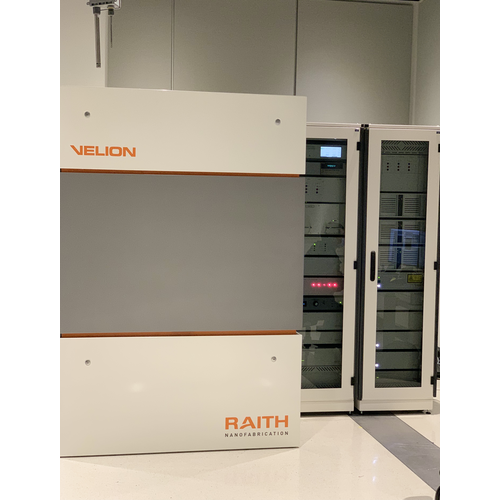 |
VELION FIB-SEM |
|
Hourly Rate : $82 |
VELION is a FIB-SEM instrument dedicated to nanofabrication where Focused Ion Beam (FIB) technology has matured into state-of-the-art instrumentation for nanofabrication and rapid prototyping. VELION comprises a top down mounted nanoFIB column perpendicular to a Laser Interferometer Stage with an attached FE SEM column. The instrument offers unique capabilities and is highly optimized for fabricating high resolution, 2D and 3D nanostructures. |
| |
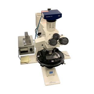 |
Zeiss Axioskop |
|
Hourly Rate : $37 |
Transmission, Reflection, T & R Polarized, Brightfield, Reflectance Differential Interference Contrast (DIC).Digital Camera, Axiovision Software |
| |
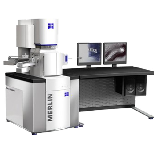 |
Zeiss Merlin High-resolution SEM |
|
Hourly Rate : $70 |
Zeiss Merlin high-resolution scanning electron microscope is a versatile electron beam characterization tool for semiconductor research, life and material sciences. It is capable of high resolution secondary electron imaging with a resolution of 0.8 nm at 15KV and 1.4 nm at 1 kV with in-lens secondary electron detector. It is also equipped with a retractable 4 Quads and an in-lens energy selective backscatter detectors for back-scattered electron imaging, an unique charge compensation system for imaging of non-conductive materials, and a scanning transmission electron microscopy (STEM) detector for studying of electron-transparent thin film samples. A software to reconstruct 3D surface topography is also available. Accessories include an EDS for X-ray microanalysis and elemental mapping and an EBSD for crystallographic texture study. |
| |
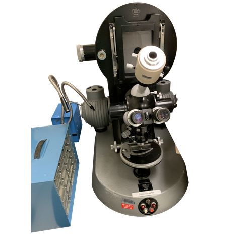 |
Zeiss Ultraphot |
|
Hourly Rate : $37 |
This is a modular microscpe built in 1934 to replace four or five micropses in the laboratory.
Transmission, Reflection, Polarized, Phase, Long Working Distance Objectives (Luminar), Xenon Lamp, Mercury Lamp |
|
|
| |
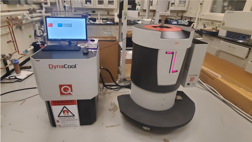 |
Dynacool PPMS |
$200.00 |
Hourly Rate : $0 |
A PPMS is used for cryogenic to room temperature measurements of sample magnetic and electrical properties including hall measurements at the most basic, with vibrating sample magnetometry and other more sophisticated measurements available with extra training.
The Quantum Design PPMS represents a unique concept in laboratory equipment: an open architecture, variable temperature-field system, designed to perform a variety of automated measurements. Available measurement options include all required hardware and electronics to immediately begin collecting publication-quality data, while the system is also easily adapted to custom user experiments. Sample environment controls include fields up to �16 T and a temperature range of 1.9 to 400K. The expandable design enables combining many features in one instrument to make the PPMS the most versatile system of its kind. |
| |
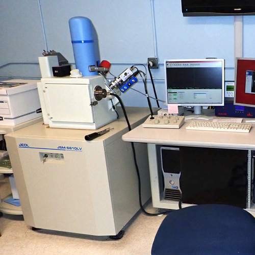 |
JEOL JSM-6610LV |
|
Hourly Rate : $52 |
The JEOL JSM-6610LV is a scanning electron microscope that can operate in High Vacuum mode or in Low Vacuum mode up to 270 Pa. It can image non-conductive samples directly without conductive coating. Detectors include an Everhart-Thornley detector for High Vacuum , a JEOL Low Vacuum secondary detector, a 3 mode backscatter detector and a 30 mm2 Silicon drift detector EDS detector. The microscope has an IXRF EDS system and a 200 N deformation stage for in-vacuum tension and compression testing. It has 30 x 30 x 30 cm chamber and is equipped with a 5 axis computer controlled positioning system. Maximum magnification is 300,000. |
| |
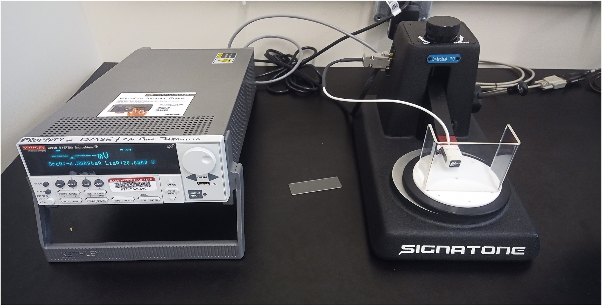 |
Pro4 Four Point Probe |
|
Hourly Rate : $10 |
A four point probe allows for measurement of surface conductivity for thin films in a quick and simple method. You may either measure the surface conductance, or if you know the film thickness you can measure the conductivity.
The Pro4 is designed to meet the demands of research on wafers, thin films, solar cells and a variety of applications.
The Pro4 employs the ASTM F84 in line four-point probe configuration. Dual configuration is also used but may be switched off if not desired. The dual configuration method may be found in the NIST publication 260-131. When calibrated with a NIST traceable standard, the accuracy through the standard range is 1%.
ASTM and NIST standards may be found in the MIT libraries for reference. |
| |
 |
Probe Station S-1160 |
|
Hourly Rate : $10 |
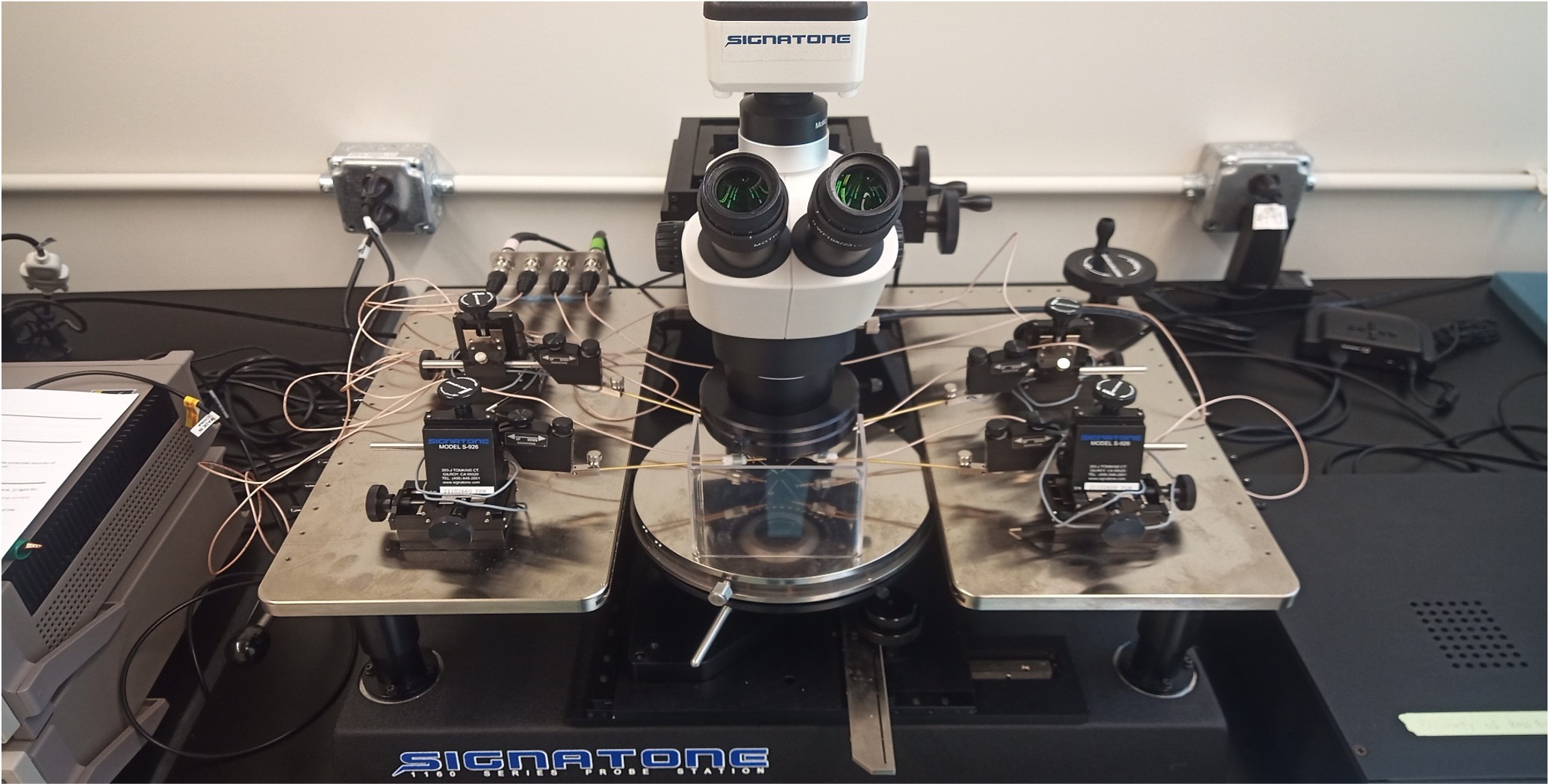
A probe station is a flexible tool used to allow for positioning both low frequency and RF probe tips to contact a fabricated sample. An example use is to measure the ferroelectric properties of a new material, to test the opto-electrical properties of a device using custom laser or LED illumination, or to characterize an antenna.
The Signatone S - 1160 150mm - 200mm Manual Probe System designed for reliable and accurate analytical testing of DC, CV-IV, and High-Power applications.
Attachments include
- Standard single tip probes
- Microwave Probes SP-40A
- Keithly 6221
- Keithly 2182A
- Premier II Ferroelectric Tester
- 8753C Network Analyzer with 85047A S-Parameter Test Set
- Optical Breadboard for attaching lasers/optics |
| |
 |
Refund |
|
Hourly Rate : $-1 |
|
| |
 |
Vibrating Sample Magnetometer |
|
Hourly Rate : $15 |
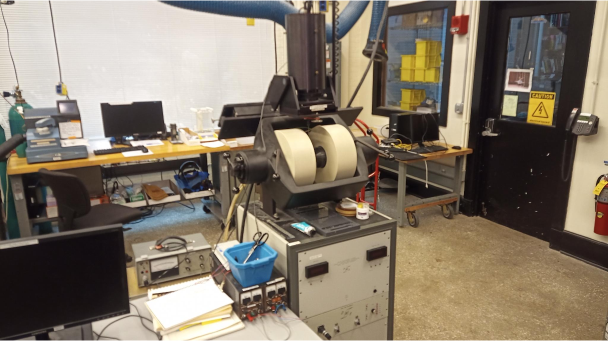
Standard system for taking cyclic magnetometry data from magnetic materials at room temperature in fields up to 10000 gauss. |
|
|
| |
 |
Differential scanning calorimetry |
|
Hourly Rate : $35 |
|
| |
 |
VCA (Video Contact Angle System) |
|
Hourly Rate : $35 |
|
| |
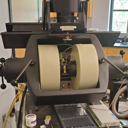 |
VSM (Vibrating Sample Magnetometer) |
|
Hourly Rate : $35 |
|
|
|
| |
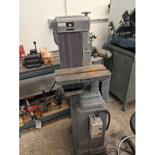 |
Belt Sander |
|
|
|
| |
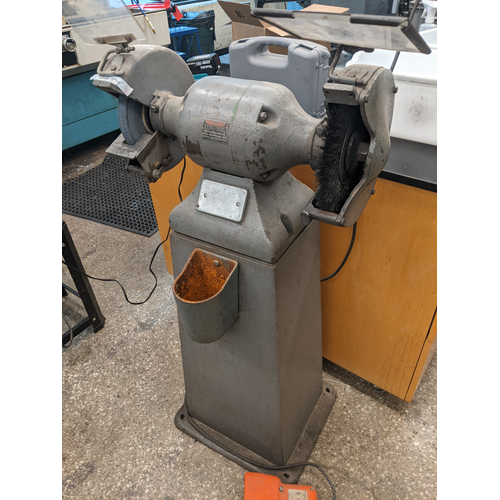 |
Bench Grinder |
|
|
|
| |
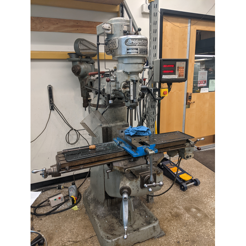 |
Bridgeport Mill |
|
Hourly Rate : $15 |
Manual milling machine |
| |
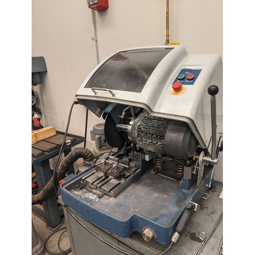 |
Buehler Abrasimet 250 |
|
|
Abrasive cutoff saw |
| |
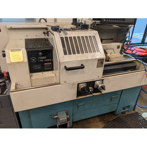 |
CNC Lathe |
|
Hourly Rate : $15 |
CNC Lathe |
| |
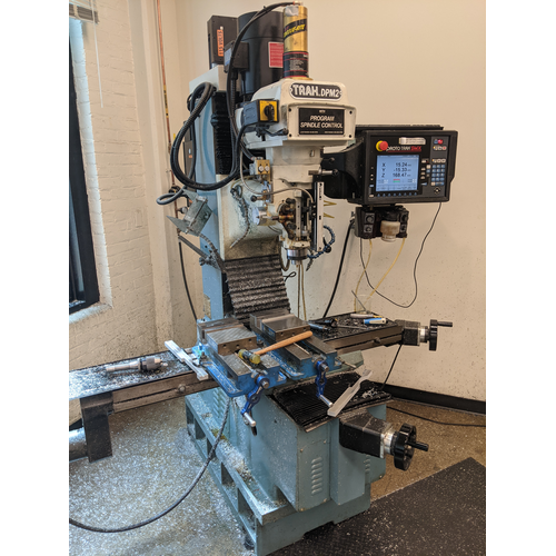 |
CNC Mill |
|
Hourly Rate : $15 |
CNC milling machine |
| |
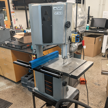 |
Delta Band Saw |
|
|
plastic and wood only |
| |
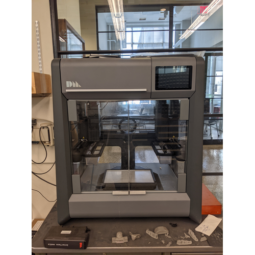 |
Desktop Metal Studio System |
|
|
Metal 3D printer |
| |
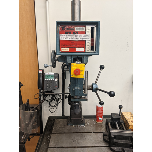 |
Drill Press |
|
|
|
| |
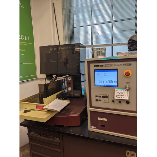 |
EDM |
|
Hourly Rate : $6 |
Wire EDM |
| |
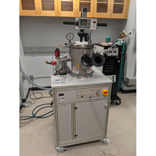 |
Edmund Buehler Arc Melter |
|
Hourly Rate : $15 |
Arc melter with suction casting |
| |
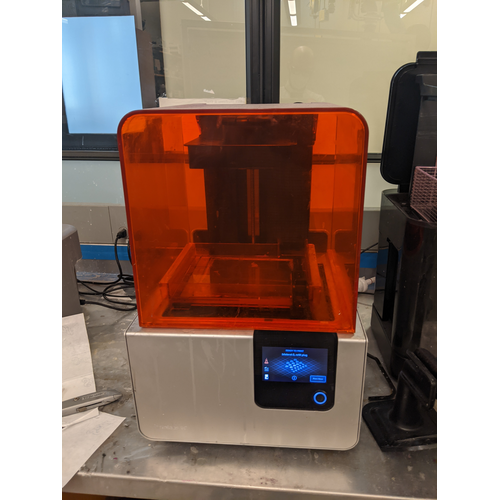 |
Formlabs Form 2 Printer |
|
Material Rates :
Castable or Flexible resins ( $0.5 per mL)
Standard Resin ( $0.25 per mL) |
SLA photopolymer 3D printer |
| |
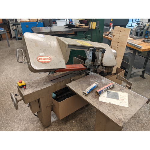 |
Kalamazoo Horitzonal Band Saw |
|
|
|
| |
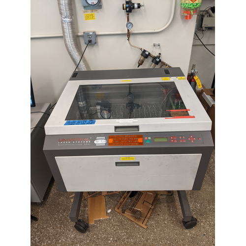 |
Laser Cutter |
|
Hourly Rate : $20 |
60 W laser cutter |
| |
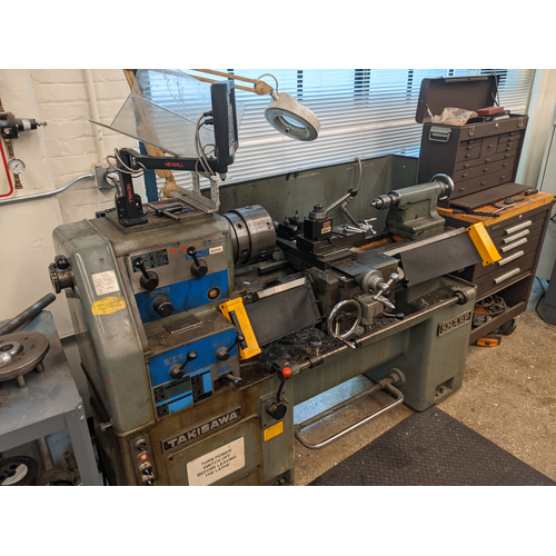 |
Manual Lathe |
|
Hourly Rate : $15 |
Manual Lathe |
| |
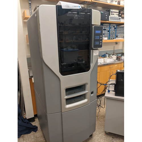 |
Stratasys Dimension BST1200es |
|
Material Rates :
ABS Plus ( $12 per Inch^3) |
ABSplus FDM printer, no soluble support, 10x10x12" build |
| |
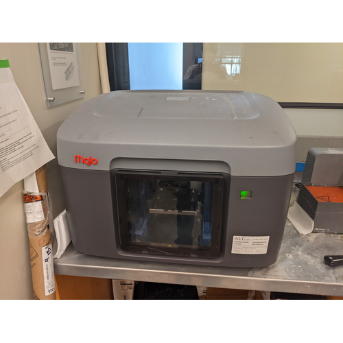 |
Stratasys MOJO 3D printer |
$10.28 |
Material Rates :
MOJO General 3D Polymaterial ( $3.75 per in^3) |
ABSplus FDM printer, soluble support, 5x5x5" build |
| |
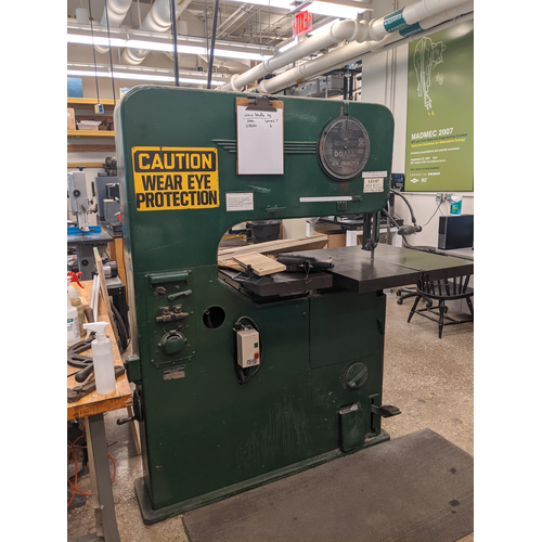 |
Vertical band saw |
|
|
metal only |
| |
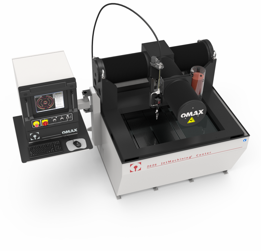 |
Waterjet |
|
Hourly Rate : $120 |
|
|
|
| |
 |
1100 C Tube Furnace |
|
Hourly Rate : $15 |
1100 C max temp |
| |
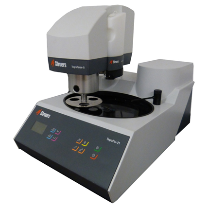 |
Automatic Grinding Machine |
|
Hourly Rate : $20 |
Manual/automatic grinding machine |
| |
 |
Automatic Hardness Tester |
|
Hourly Rate : $35 |
Vickers hardness tester with motorized stage. |
| |
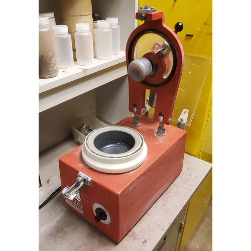 |
Automatic Mortar/Pestle |
|
Hourly Rate : $15 |
Automatic mortar and pestle. Agate bowl. |
| |
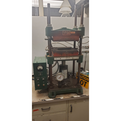 |
Carver Hot Press |
|
Hourly Rate : $0 |
Hot Uniaxial Press |
| |
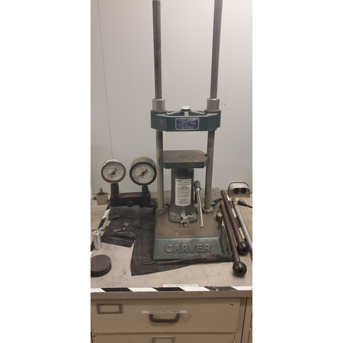 |
Carver Press |
|
|
Uniaxial Press |
| |
 |
Cold Mounting Station |
|
Hourly Rate : $20 |
Area for encapsulation of specimens in epoxy for subsequent grinding/polishing. Epoxy resin, molds, specimen stands, etc. supplied. |
| |
 |
Electrolytic Polisher/Etcher |
|
Hourly Rate : $20 |
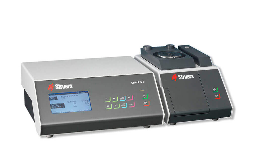
Electrolytic Polisher/Etcher. Currently cannot use etchants containing perchloric acid. |
| |
 |
Hadur - Vacuum Pressing Furance |
|
Hourly Rate : $40 |
This machine is designed for making dense compound materials under both vacuum and high pressure up to 2 metric tons. It is integrated with a split vertical tube furnace with a vacuum-sealed 4" quartz tube and 2000Kg digital electric press, as well as one set of 0.5" ID graphite pressing dies. The furnace can be heated up to 1000 C using a temperature controller with 30 programmable segments. Water-cooled flanges facilitate a vacuum with a mechanical pump. |
| |
 |
Hardness Tester (8-102, Older Unit) |
|
Hourly Rate : $35 |
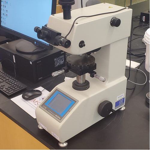
Vickers/Knoop microhardness tester |
| |
 |
Hardness Tester (Newer Unit) |
|
Hourly Rate : $35 |
|
| |
 |
Helios - 1800 C Tube Furnace |
|
Hourly Rate : $40 |
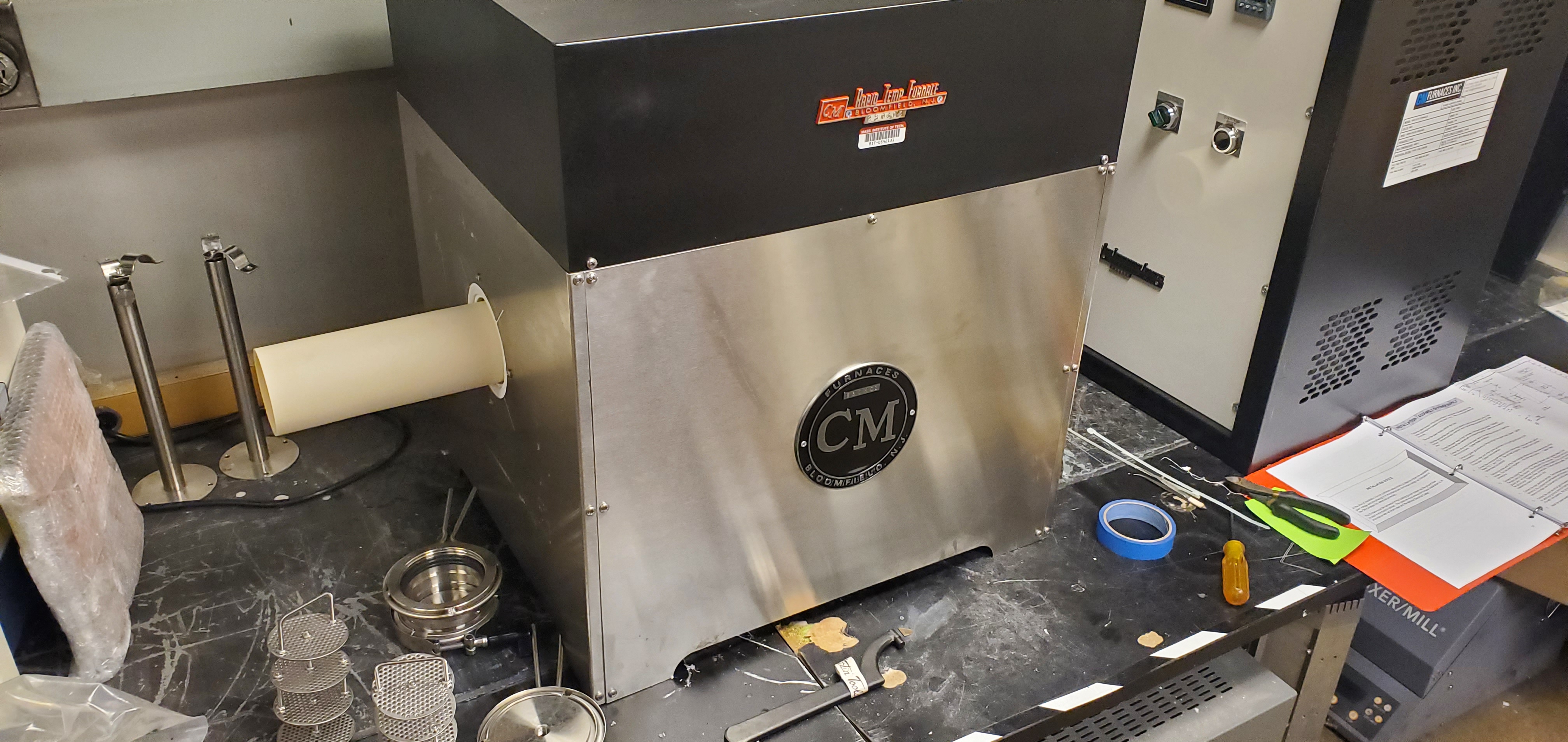
High temperature tube furnace (1800 C max temp) for inert and oxidizing atmospheres. |
| |
 |
High Energy Ball Mill |
|
Hourly Rate : $15 |
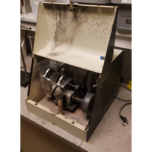
Users must provide their own jar(s). |
| |
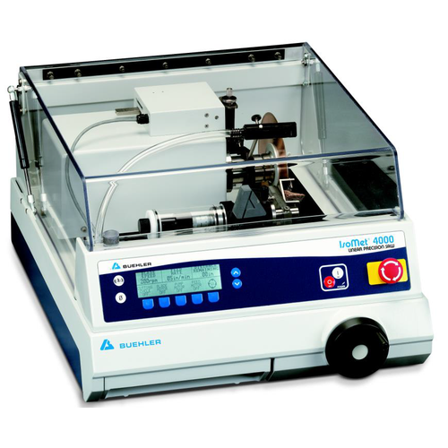 |
High Speed Saw |
|
Hourly Rate : $20 |
Precision Diamond Saw |
| |
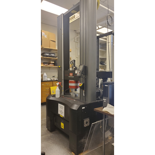 |
Instron (150kN Unit) |
|
Hourly Rate : $30 |
150 kN capacity |
| |
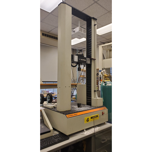 |
Instron (5kN Unit) |
|
Hourly Rate : $30 |
5 kN capacity |
| |
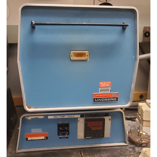 |
Large Box Furnace (1000 C) |
|
Hourly Rate : $15 |
1000 C Max temp |
| |
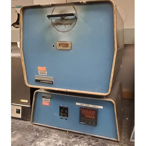 |
Large Box Furnace (1200 C) |
|
Hourly Rate : $15 |
1200 C Max Temp |
| |
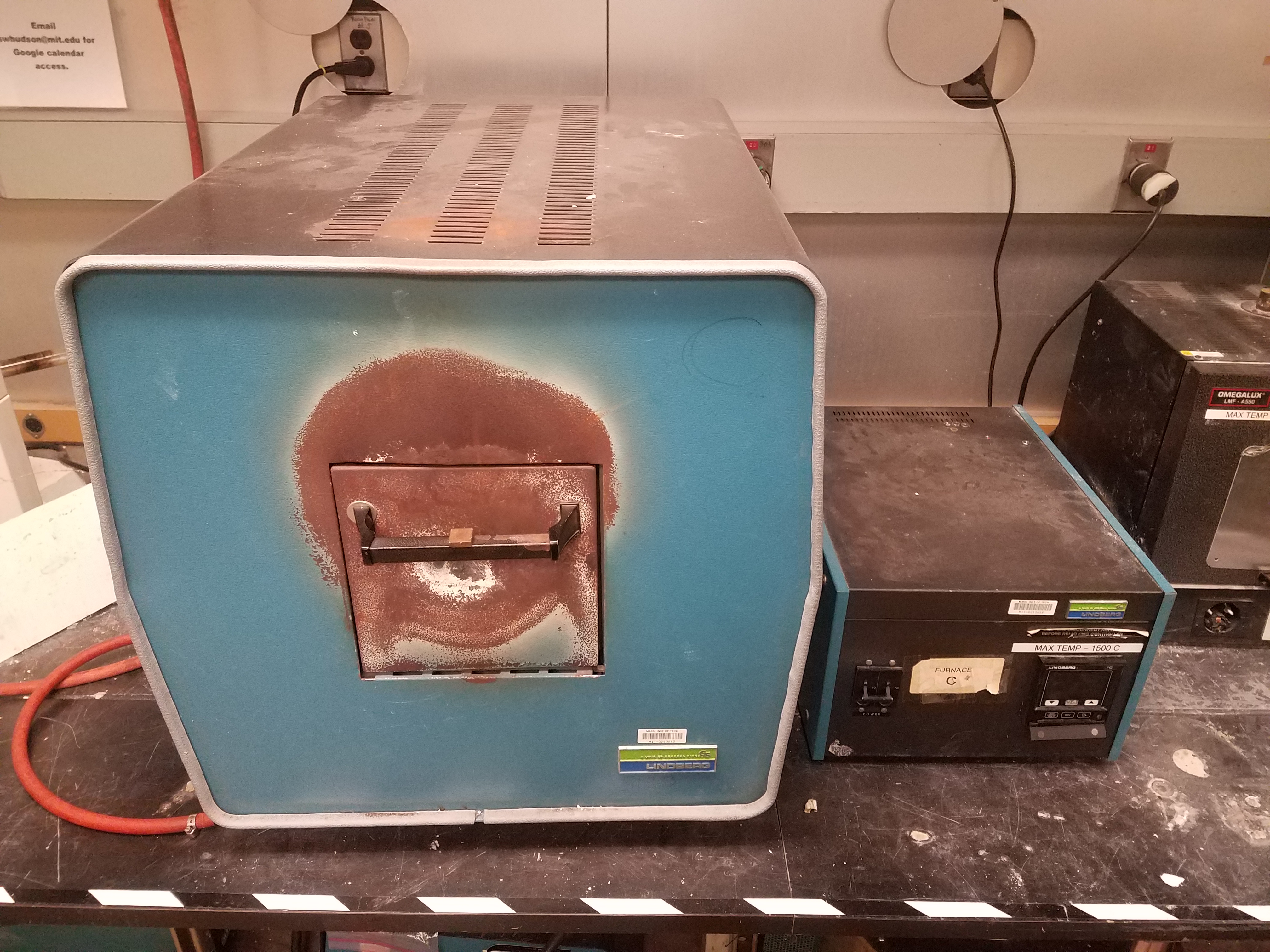 |
Large Box Furnace (1500 C) |
|
Hourly Rate : $15 |
Box Furnace (1500 C Max Temp) |
| |
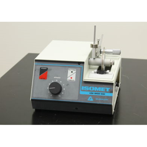 |
Low Speed Saw |
|
Hourly Rate : $20 |
Precision Diamond Saw |
| |
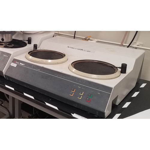 |
Manual Grinding Machine |
|
Hourly Rate : $20 |
Manual grinder/polisher |
| |
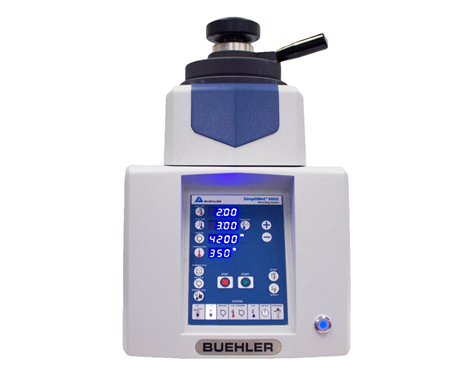 |
Mounting Machine (Buehler Unit, 1.25 in. puck) |
|
Hourly Rate : $20 |
Hot mounting machine (1.25 in. pucks) |
| |
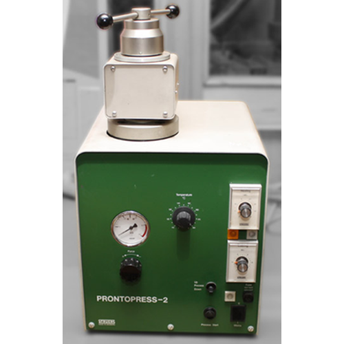 |
Mounting Machine (Struers Unit, 1.5 in. puck) |
|
Hourly Rate : $20 |
Hot mounting machine (1.5 in. pucks) |
| |
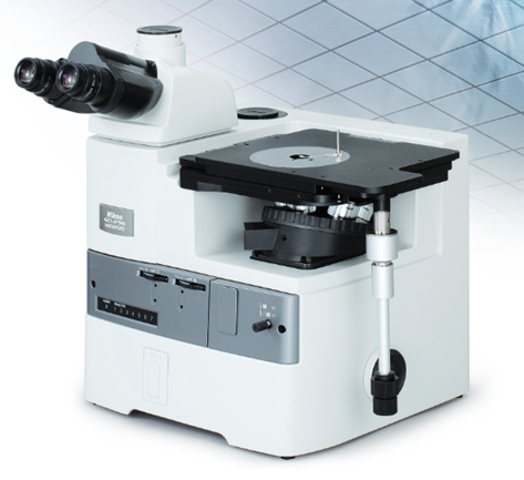 |
Nikon MA200 Microscope |
|
Hourly Rate : $20 |
Inverted metallurgical microscope. 50-2000x |
| |
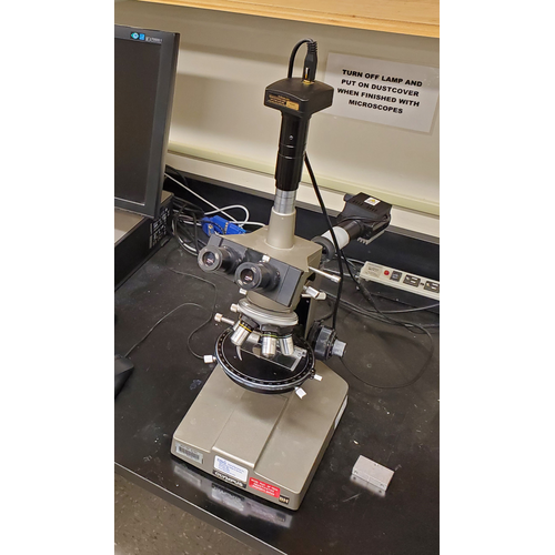 |
Olympus BH2 Microscope |
|
Hourly Rate : $20 |
Microscope
|
| |
 |
Oxy-Hydrogen Torch/Quartz ampoule encapsulation |
|
Hourly Rate : $45 |
Bench for making quartz ampoules. Torch, tools, and quartz stock supplied. |
| |
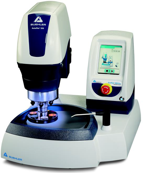 |
Polishing Machine |
|
Hourly Rate : $20 |
Polishing machine |
| |
 |
Polishing Machine (With Dosing Pump) |
|
Hourly Rate : $20 |
Polishing machine with dosing pump |
| |
 |
Refund |
|
Hourly Rate : $-1 |
|
| |
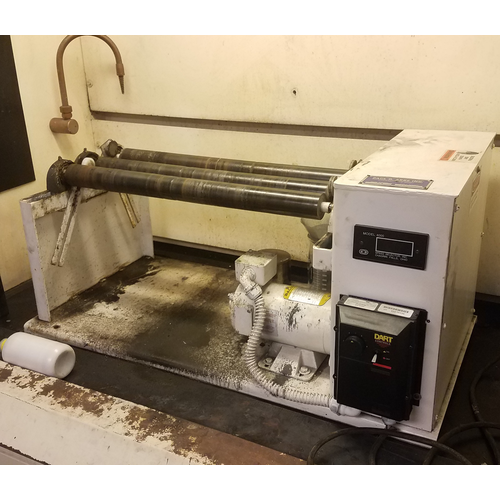 |
Rolling Ball Mill |
|
Hourly Rate : $15 |
Users must provide their own jar(s). |
| |
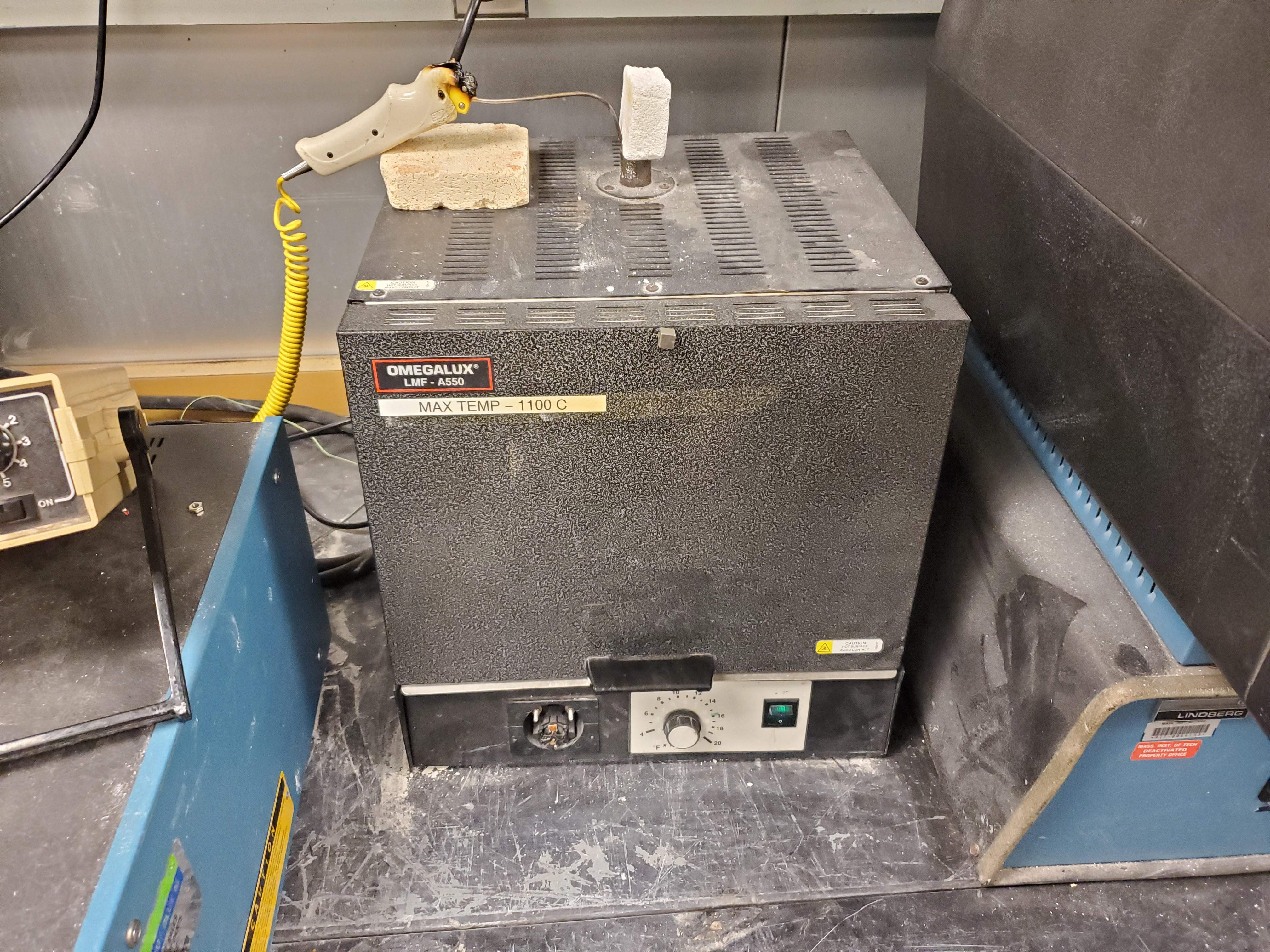 |
Small Box Furnace (1100 C) |
|
Hourly Rate : $15 |
Box Furnace (1100 C Max Temp) |
| |
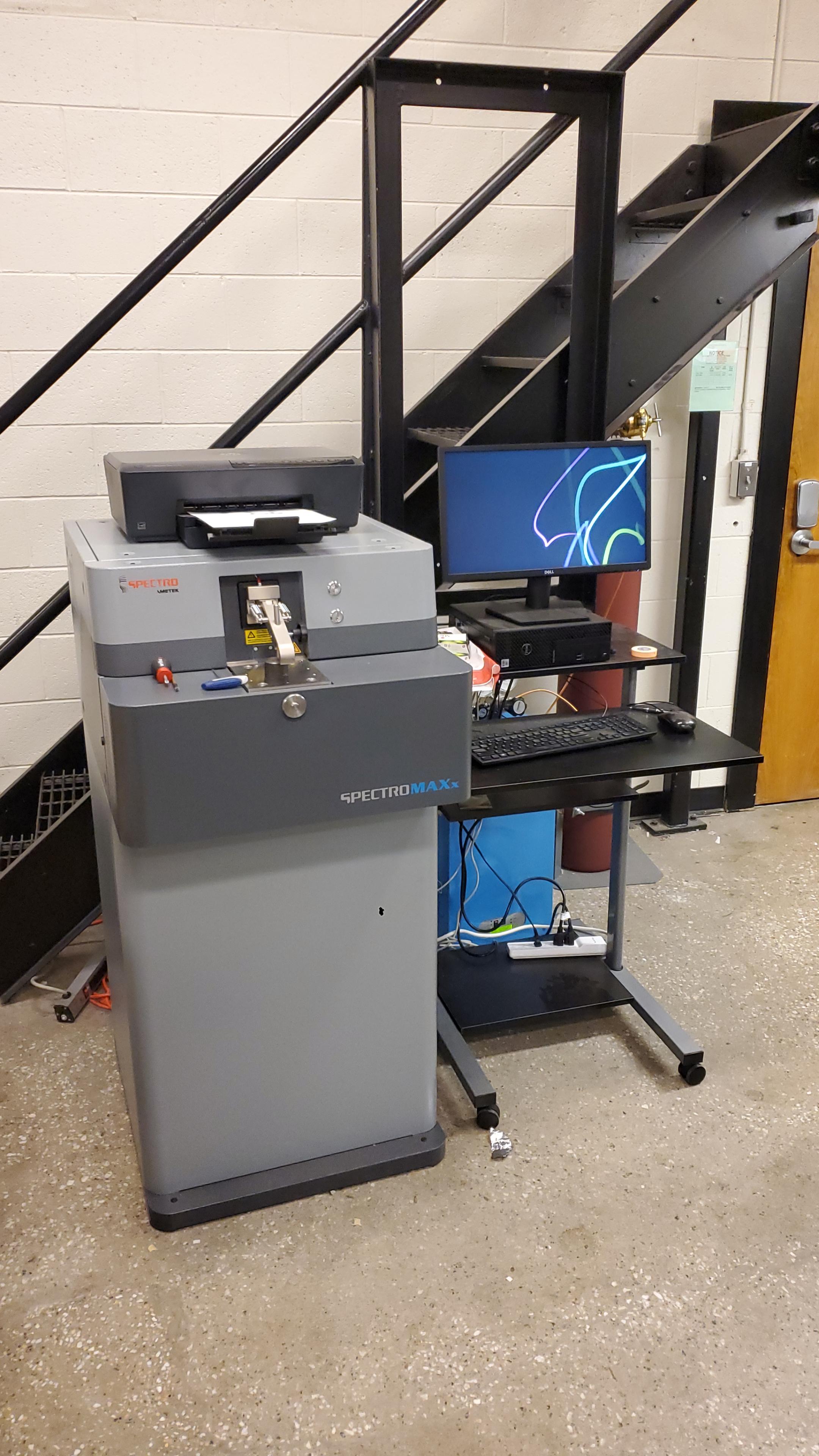 |
Spark OES |
|
Hourly Rate : $40 |
Stationary spark optical emission spectrometer (spark-OES). Used for bulk composition measurement of Fe, Al, Cu, Ti, Co, and Ni alloys. |
| |
 |
Swab/Immersion Etching Area |
|
Hourly Rate : $20 |
Currently cannot use etchants containing perchloric acid. |
| |
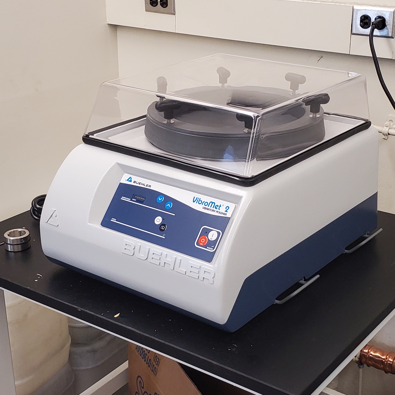 |
Vibratory Polisher |
|
Hourly Rate : $40 |
Vibratory polisher geared toward preparation of EBSD/ECCI quality surfaces. Excellent for soft metals, composites, and delicate specimens. Additional specimen holders enable TEM sample prethinning and fine material removal for fabrication. |
| |
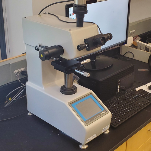 |
Vickers/Knoop Hardness Tester |
|
Hourly Rate : $35 |
Vickers/Knoop microhardness tester |
| |
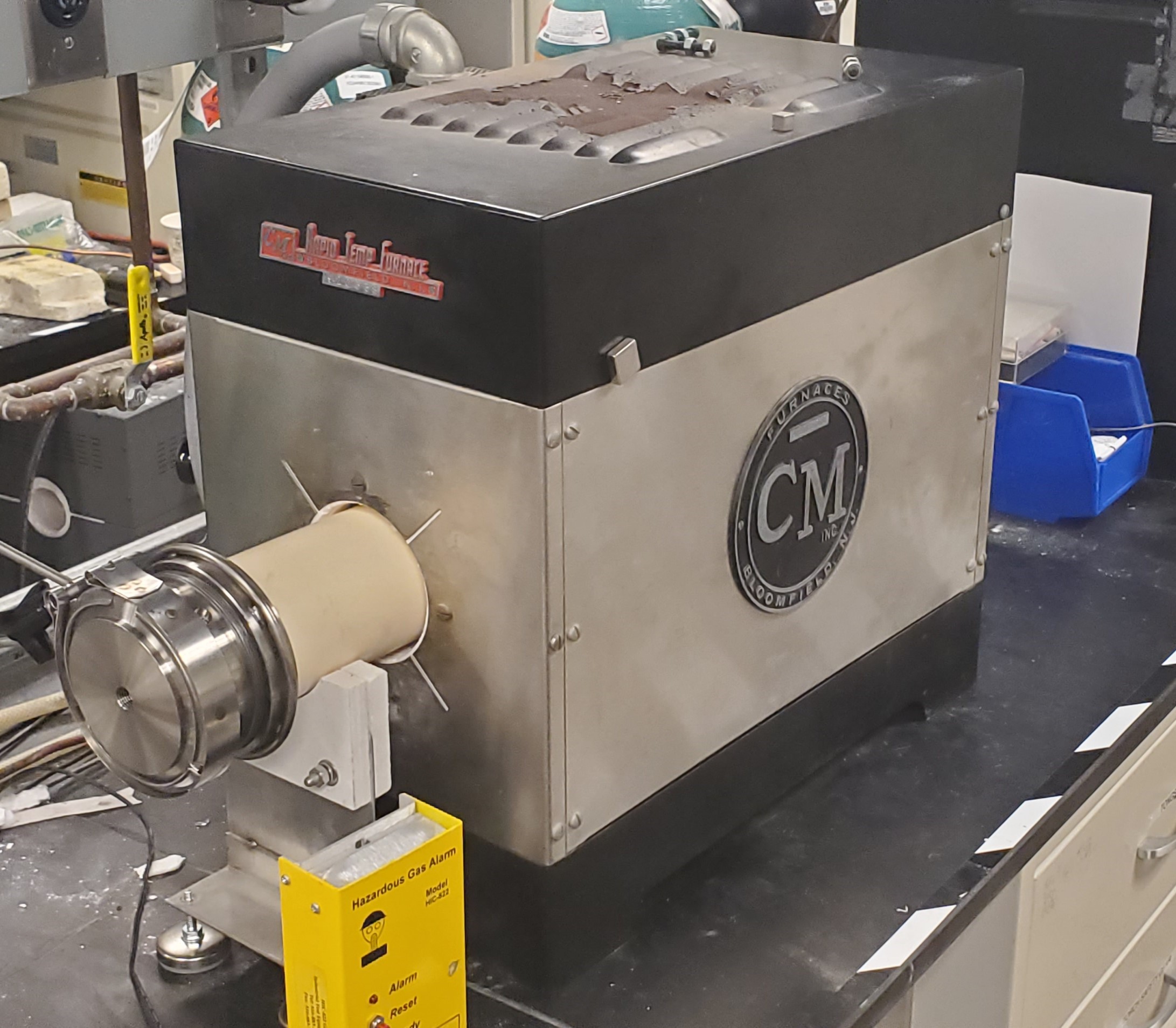 |
Vulcan - Hydrogen Tube Furnace |
|
Hourly Rate : $40 |
1600 C max temp. Built for running in a hydrogen or forming gas (Ar+H2 mix) environment. |
|
|
| |
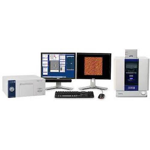 |
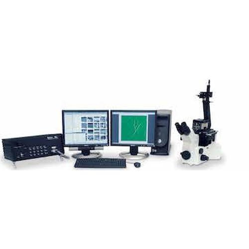
Asylum Research Cypher S AFM |
|
Hourly Rate : $70 |
This high-resolution atomic force microscope (AFM) with a standard scanner has a bandwidth of up to 8 MHz, which makes it well-suited for multifrequency modes, such as Dual AC and AM-FM. Other techniques include EFM, KPFM, MFM, LFM, force spectroscopy and tapping mode. For well-prepared surfaces, high speed imaging up to 20 Hz is feasible. Raster scans down to 200 nm is routine. |
| |
 |
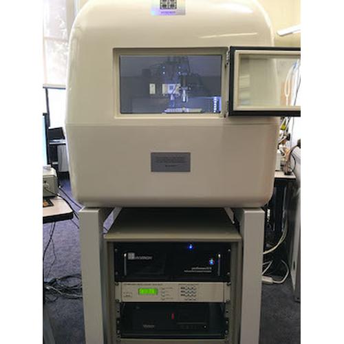
Asylum Research MFP-3D Bio AFM |
|
Hourly Rate : $70 |
This atomic force microscope (AFM) can be used as a standard AFM, though its bandwidth is limited to 1 MHz. Generally, half micron scans are feasible. However, its unique advantage is force microscopy in a fluid environment. Measured and applied forces range from tens of picoNewtons to nanoNewtons. Typical samples for force microscopy in a fluid environment are hydrogels and biological cells. |
| |
 |
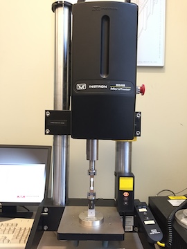
Bruker TriboIndenter 950 |
|
Hourly Rate : $70 |
This Hysitron product from Bruker Corporation is a very sensitive nanoindenter that can apply and measure forces from 10 microNewtons to 10 milliNewtons. Likewise, it can apply and measure displacements from tens of nanometers to 5 microns. In addition to quasistatic indentation, scratching, lateral force and friction measurements, and cyclic loading, it also has the ability to do dynamic mechanical measurements up to 300 Hz at room temperature only. Lastly, the nanoindenter can be used as a scanning probe microscope to generate topographical images of the surfaces before and after indentation. |
| |
 |
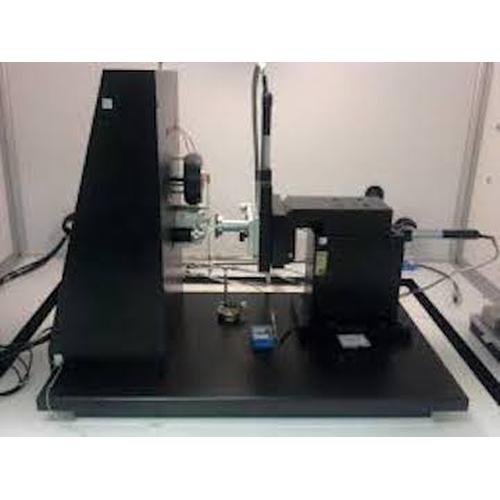
Instron MicroTester 8848 |
|
Hourly Rate : $70 |
This table-top electromechanical universal tension/compression apparatus, made by Instron Corporation, can be used for uniaxial testing of small and thin materials. It can apply and measure loads ranging from 1 to 2000 Newtons. Typical samples range from elastomers to metal alloys. |
| |
 |
Micro Materials NanoTest NTX |
|
Hourly Rate : $70 |
This micro/nanoindenter is capable of measuring and applying loads and depths ranging from 1 milliNewton to 20 Newtons and up to 70 microns respectively. Quasistatic indentation, scratching, lateral force and friction measurements, cyclic loading, impact testing and dynamic hardness measurements are all possible, both in air and liquid. |


